GPU architecture describes how a graphics processing unit (GPU) is designed to process many calculations in parallel, including how its cores, memory, interconnects, and specialized accelerators work together. GPU architecture can be understood in two ways:
- Chip-level GPU architecture: the internal blueprint of a GPU, including its cores, memory hierarchy, execution model, and specialized accelerators that enable highly parallel computation
- Rack-scale GPU architecture: the design of multi-GPU systems at the data center level, including interconnects, cooling, and power delivery that determine how GPUs scale in production environments
Both perspectives matter. Chip-level architecture defines the raw performance of a GPU, while rack-scale architecture dictates how effectively GPUs can be deployed at scale for AI, HPC, and other compute-intensive workloads.
Unlike a CPU, which is generally optimized to execute a relatively small number of complex instruction streams with low latency, a GPU prioritizes throughput by keeping many lightweight threads in flight and applying similar operations across large datasets in parallel.
Originally built for rendering images and graphics, modern GPU architectures have evolved to power advanced workloads in artificial intelligence (AI), high-performance computing (HPC), scientific simulations, and more. Whether you’re training a large language model or running a weather forecast simulation, the underlying GPU architecture dictates performance, scalability, and efficiency.
In the sections that follow, you’ll learn:
- The key components that make up chip-level GPU architecture
- How modern GPU architectures differ, using the NVIDIA Ada Lovelace, Hopper, Blackwell, and Vera Rubin platforms as examples
- Why rack-scale GPU architecture is critical for data center deployments
- The innovations and challenges shaping today’s GPU landscape
- How GPU architecture impacts real-world use cases in AI, HPC, and beyond
What are the main components of GPU architecture?
At the most basic level, GPU architecture refers to the internal design of the GPU: the way its cores, memory, and processing pipelines are structured to handle massive amounts of data in parallel, often executing thousands of operations simultaneously.
This high level of parallelism is possible because the GPU contains many arithmetic execution lanes organized into larger compute units. It also maintains many active threads so that useful work can continue while others wait for data or instructions.
Key aspects of the GPU make this parallel computing possible, including the processing units, execution models, memory, specialized cores, and scalable interconnects.
Processing units
Processing units are the fundamental compute elements of a GPU responsible for performing mathematical operations on data and grouping cores for parallel processing. This is a fundamental difference from CPUs, which typically use fewer, more general-purpose cores optimized for latency-sensitive serial work.
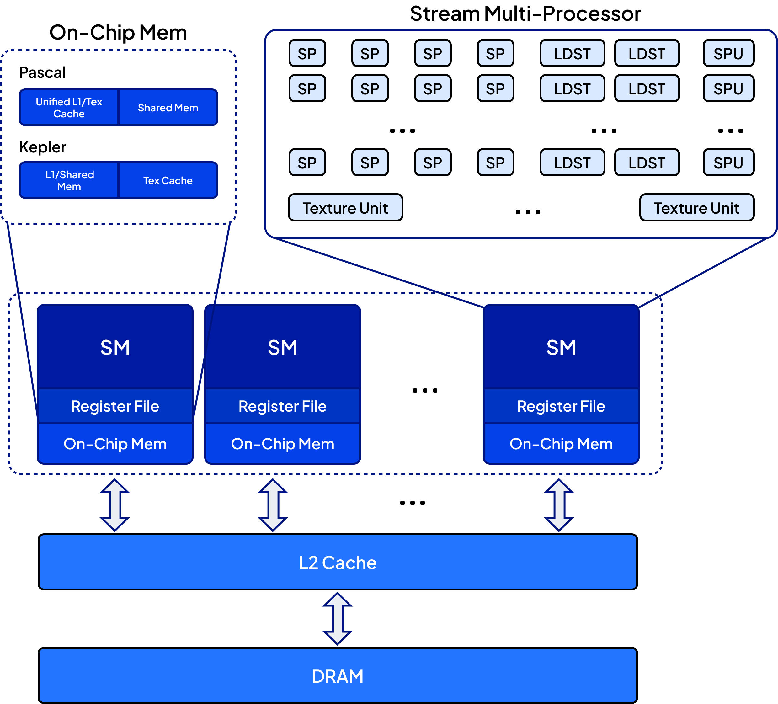
In NVIDIA GPU architectures, processing units are grouped into Streaming Multiprocessors (SMs), each containing hundreds of cores that execute thousands of threads simultaneously. For example, an NVIDIA H100 configuration can include many Streaming Multiprocessors, each with CUDA cores and tensor cores that execute large numbers of parallel operations. In total, they can execute hundreds of thousands of threads concurrently.
Execution models
Execution models define how the GPU schedules and processes instructions across many threads. Modern GPUs expose a SIMT (Single Instruction, Multiple Threads) programming model on top of SIMD (Single Instruction, Multiple Data) hardware , which allows multiple threads to execute the same instruction on different data in parallel.
Memory hierarchy
High-bandwidth memory and large caches ensure data moves quickly between compute units and storage. The layered memory structure within a GPU—ranging from on-chip registers and caches to high-bandwidth external memory—determines how efficiently data can be moved and reused during computation.
At a high level, the hierarchy moves from fast, small on-chip registers and shared memory through L1 and L2 caches to larger off-chip HBM or GDDR memory. Keeping frequently reused data closer to the execution units can reduce latency and improve performance.
Over the past few years, GPU memory has become increasingly important to the performance and scalability of AI workloads. For AI workloads, high-bandwidth memory such as HBM can be more important than raw compute alone because large models must constantly move parameters, activations, and intermediate results between memory and compute units.
Specialized cores
Beyond general-purpose compute cores, modern GPUs incorporate dedicated hardware units designed for specific types of computation. These include tensor cores for AI workloads, transformer engines for large language models, and RT cores for real-time ray tracing.
For example, NVIDIA Hopper architecture transformer engine dynamically switches between FP8 (8 bit Floating Point) and FP16/BF16 (Brain Floating Point) precision to accelerate transformer-based models, achieving up to 4x faster training on large-scale generative AI workloads.
Scalable interconnects
Interconnect technologies link multiple GPUs together to share data quickly, reducing communication overhead and improving distributed training efficiency.
NVIDIA NVLink™ and NVLink Switch allow GPUs in a cluster to communicate at hundreds of GB/s—critical for training massive foundation models like LLaMA or Gemini across multi-node systems.
All together, this architecture allows GPUs to quickly move vast amounts of data and perform trillions of operations in parallel, making them uniquely suited to AI and other compute-intensive workloads. Here’s how the pieces fit together:
Examples of modern GPU architectures
NVIDIA architectures provide useful examples of how GPU design has evolved for graphics, AI, and HPC workloads. This section uses NVIDIA as an example while keeping the architectural concepts applicable across cloud and data center environments. Each generation reflects advances not only in silicon performance but also in how GPUs are optimized for specific workloads: real-time rendering, large-scale neural networks, or data-center-scale simulations.
Early GPU architecture laid the foundation for parallel compute and deep learning acceleration. But as AI models grew from millions to trillions of parameters, NVIDIA’s more recent architectures—including NVIDIA Rubin—have focused on increasing memory bandwidth, improving interconnect speed, and introducing specialized cores for transformer-based workloads.
These designs illustrate how GPU architecture has evolved from pixel rendering pipelines to full-stack compute platforms, capable of powering everything from cinematic ray tracing to foundation-model training.
NVIDIA GPU architectures
Each of NVIDIA’s most recent GPU architectures reflects different priorities, whether enabling immersive visual experiences, accelerating AI model training, or scaling scientific workloads across thousands of GPUs.
NVIDIA Ada Lovelace
Optimized for visual computing, Ada Lovelace introduced major leaps in energy efficiency and graphics performance. Built on the TSMC 4N process, it supports GDDR6X memory, 3rd-generation RT cores, and 4th-generation tensor cores.
NVIDIA Hopper
Designed for AI and HPC, Hopper redefined GPU compute with the introduction of the Transformer Engine and HBM3 memory. It features NVLink 4.0 for high-bandwidth multi-GPU scaling and introduces native support for FP8 precision, enabling faster, more efficient deep-learning training.
NVIDIA Blackwell
Blackwell extends Hopper’s AI-focused design with a dual-die GPU architecture, second-generation Transformer Engine capabilities, FP4/NVFP4 support, high-bandwidth HBM3e memory, and fifth-generation NVLink for large-scale AI training and inference.
NVIDIA Rubin
Vera Rubin is NVIDIA’s next-generation AI infrastructure platform, designed around rack-scale systems that combine Rubin GPUs, Vera CPUs, sixth-generation NVLink, networking, DPUs, and system-level resiliency for agentic AI and long-context workloads.
Together, these architectures illustrate how GPU design has advanced at both the chip and system levels. Each new generation refines the internal balance of cores, memory, and specialized engines.
However, true performance depends on how those GPUs are deployed, interconnected, and cooled in production environments. In other words, the chip-level architecture is only half the story; the other half lies in the rack-scale architecture that determines how GPUs work together at scale.
Rack-scale GPU architecture and why it matters
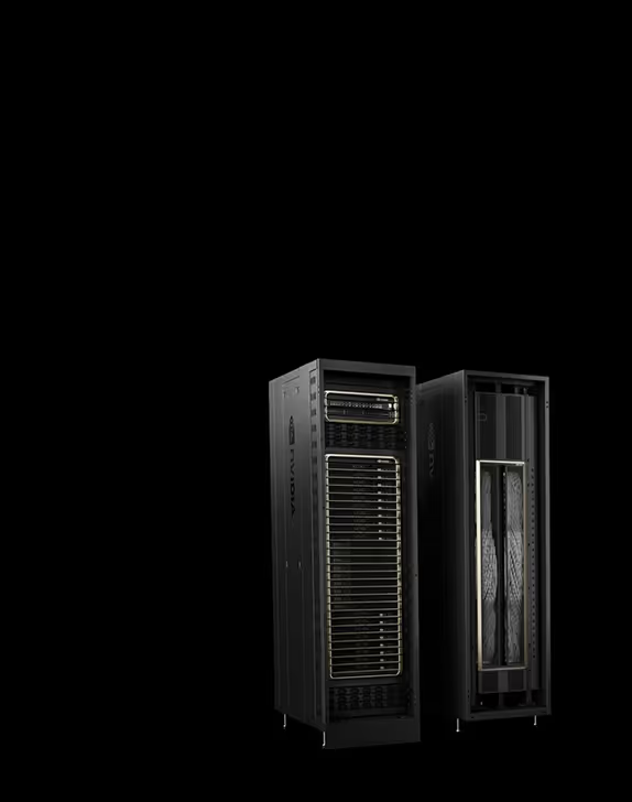
When we shift from individual GPUs to multi-GPU systems in data centers, a new set of design concerns arises. Rack-scale GPU architecture defines how GPUs, CPUs, networking, storage, and cooling are organized, interconnected, and managed as a unified compute system.
Performance at this scale is shaped not just by the power of a single GPU but by how efficiently tens to thousands of GPUs communicate, share memory, and maintain thermal stability under load. Bandwidth, latency, and data locality become as critical as core counts or clock speeds, since bottlenecks in interconnects, power delivery, or memory can negate the raw performance advantages of advanced architectures like Hopper or Blackwell. In short, the rack itself becomes part of the GPU architecture.
Below is an expanded list of the major components and considerations that influence both performance and scalability in rack-scale GPU design:
- Connectivity: the interconnect network fabric linking GPUs (and CPUs) inside a rack that determines how quickly data can be shared; this includes NVLink, NVSwitch, PCIe, NVIDIA Quantum InfiniBand, and RDMA over Converged Ethernet (RoCE)
- Intra-node connectivity: the high-speed interconnect fabric linking GPUs and CPUs within a single server node (including NVLink, NVSwitch, and PCIe), which determines how quickly data moves between chips on the same board or system
- Inter-node and cluster networking: the fabric linking nodes across a rack or cluster, including Quantum InfiniBand and RDMA over Converged Ethernet (RoCE), which determines cross-node bandwidth and latency at scale
- Storage: this includes not only the GPUs’ VRAM (HBM, GDDR) but also shared memory systems (e.g. CPU memory, pooled memory, remote memory), local NVMe / SSD storage, and networked storage systems (disaggregated storage) that affect data locality, paging, and I/O bottlenecks
- Power delivery: the design of power distribution (e.g. PDUs, power shelves, DC vs AC, redundant paths) that can sustain high wattage per rack with headroom for peak loads
- Thermal management: liquid cooling (direct-to-chip, immersion, cold plates), in-row or in-rack coolant distribution units, airflow path design, heat exhaust, and thermal balancing across trays
- Rack topology and modular trays: how compute nodes, interconnect switch modules, and power/cooling trays are arranged physically within the rack (e.g. compute trays, switch trays, power trays), including cable routing, backplanes, and blind-mate connectors
- Management, monitoring, and orchestration: systems for telemetry, fault detection, job scheduling, GPU partitioning, and health-based failover across nodes and racks
These components work synergistically: bottlenecks, limitations, or flaws in any one can severely limit overall performance.
Evolution of rack-scale architecture
Over time, rack-scale GPU architectures have progressed in response to changes in GPU design, workload demands, and data center constraints. Below is a distilled narrative of this evolution:
Over time, rack-scale GPU architectures have progressed in response to changes in GPU design, workload demands, and data center constraints. Below is a distilled narrative of this evolution:
Early multi-GPU clusters (air-cooled, PCIe fabric)
In earlier generation systems, you would see 2–8 GPUs per server/node connected via PCIe and sometimes NVLink, with external Quantum InfiniBand for cross-node traffic. Cooling and power were relatively modest (tens of kW per rack), so air cooling sufficed, and interconnect latency dominated scaling challenges.
NVIDIA DGX SuperPOD (NVLink + NVLink Switch, denser cooling)
NVIDIA DGX systems use internal NVLink and NVSwitch fabrics, along with denser rack designs, for at-scale deployments using the NVIDIA DGX SuperPOD reference architecture. For example, a DGX SuperPOD with DGX H100 systems connects multiple DGX H100s via Quantum InfiniBand and NVLink switch fabrics.
Power densities grew (e.g. 30–50 kW+ per rack), pushing data centers to consider moving from air cooling to early liquid- or hybrid cooling solutions. NVSwitch modules were often added as dedicated switch trays to allow high-bandwidth all-to-all interconnect inside a rack.
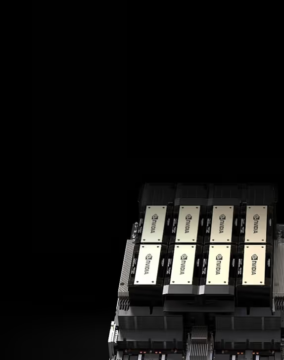
Here’s a visual example of a traditional 8-GPU architecture.

Exascale single-rack designs (GB200 NVL72 / Blackwell era)
NVIDIA Blackwell marked a new era in rack-scale design, pushing the performance, efficiency, and scalability of GPU architecture to new heights. The NVIDIA GB200 NVL72, a flagship GPU architecture of this era, merges 72 Blackwell GPUs and 36 Grace CPUs into a single NVLink domain in one rack, effectively acting as a giant monolithic GPU.
The NVIDIA GB200 NVL72 uses fully liquid-cooled trays, a modular layout of compute trays, NVLink switch trays, and power racks. The rack is engineered for ~132 kW power and dense thermal management. The system supports 130 TB/s of internal GPU communication bandwidth, leveraging 5th-generation NVLink and NVSwitch. To maintain serviceability and modularity, the rack is composed of ~18 compute trays (each 1U) plus ~9 NVLink switch trays, and power trays.
This rack-level evolution mirrors how GPU chip architecture evolved: greater density, more specialized interconnects, and tighter integration.

H100-based rack systems vs GB200 NVL72
Below is a conceptual comparison to show how modern rack-scale GPU infrastructure has evolved. (Because the public specs for H100 racks are more varied, this is illustrative.)
Architectural innovations and challenges
GPU architecture has advanced rapidly, introducing specialized features that make accelerated computing possible at scale:
- CUDA programming model (NVIDIA): a parallel computing platform that lets developers tap into thousands of GPU cores for AI, HPC, and graphics workloads
- Tensor and matrix cores: purpose-built engines for accelerating AI training, inference, and scientific workloads
- Scalable interconnects: technologies like NVLink (NVIDIA) link GPUs together, supporting faster communication and multi-GPU scaling
- Mixed-precision computing: flexible support for FP64, FP32, FP16, BF16, and FP8 formats to balance accuracy with efficiency in AI workloads
At the same time, GPU architecture can introduce operational challenges that organizations must plan for:
- Memory limits: large AI models can exceed available VRAM, leading to bottlenecks or out-of-memory errors
- Power and cooling: high-performance GPUs consume significant energy and require advanced thermal management
- Software compatibility: GPU architecture choices affect driver versions, CUDA or ROCm support, framework compatibility, container images, libraries, and workload portability across environments
- Supply chain constraints: with GPUs in consistently high demand, teams may need to plan ahead for capacity and procurement when building or scaling infrastructure
- System reliability: distributed GPU jobs are vulnerable to node failures, communication errors, or preemptions in cloud environments
Organizations adopting the latest GPU architectures must balance these innovations with careful planning to ensure efficiency, reliability, and long-term scalability.